Pulsed Growth of Vertically Aligned Nanotube Arrays with Variable Density
J. J. Jackson,‡ A. A. Puretzky,† K. L. More‡, C. M. Rouleau,† G. Eres,‡ and D. B. Geohegan†
†Center for Nanophase Materials Sciences and ‡Materials Science and Technology Division, Oak Ridge National Laboratory, Oak Ridge, Tennessee 37831-6488, United States
PDF of article published in ACS Nano 4, 7573 (2010).
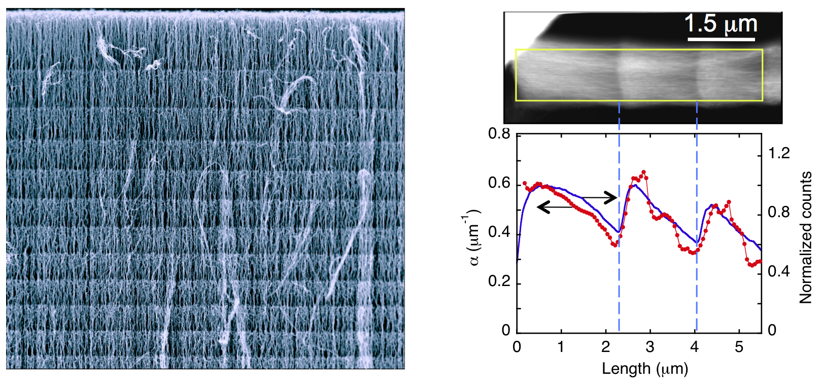
(a) Vertically-aligned carbon nanotube arrays grown by pulsed-CVD can exhibit density variations up to a factor of 1.6 within discrete 1−2 μm long layers, visible as gradient bands in SEM images of cleaved arrays and resulting in new array architectures with controllable length and density. (b) Z-contrast STEM imaging of strands of the array was used to unambiguously measure these density variations, plotted in (c) blue curve. Real-time optical reflectivity measurements of the optical extinction coefficient of the array (c), red curve, were found to provide an in situ diagnostic of this evolution in density.
Summary
When grown in high areal density on substrates, nanotubes and nanowires can form freestanding aligned architectures with exceptional thermal and electrical properties relevant to energy applications. These properties critically depend on the density of the nanomaterials, which is currently not monitored or controlled. Here, a real-time optical reflectivity method was developed to measure both the rate of growth of nanotube arrays by chemical vapor deposition, and the evolution of their density. The in situ diagnostics revealed significant density declines in the arrays as typically grown, but also a flux dependence to the array density. Pulsing the growth gas was found to repeatedly reactivate catalyst nanoparticles to increase array density, leading to a new pulsed chemical vapor deposition method to synthesize nanotube architectures with variable and controllable density.
Impact
The ability to measure both growth kinetics and density of nanomaterials in real-time provides the means to understand their growth mechanisms, as well as develop new nonequilibrium synthesis and processing approaches. Here, pulsed-CVD was developed and shown to provide a means to control two of the key issues currently limiting the application of aligned architectures of nanomaterials in technology: the need for "digital" control over length, and a pathway to increase and control their density.
Credit - This work was published in ACS Nano 4, 7573 (2010) . Research was sponsored by the Materials Sciences and Engineering Division, Office of Basic Energy Sciences, U.S. Department of Energy. Z-STEM measurement of nanotube density was conducted at the Center for Nanophase Materials Sciences, and HRTEM was performed in the Shared Research Equipment User Facility, which are sponsored at Oak Ridge National Laboratory by the Scientific User Facilities Division, U.S. Department of Energy. We gratefully acknowledge David Joy for help with microscopy estimations of densities.